Miniaturized, High Performance, Energy-and-Area-Efficient Field-Effect Transistor Expands Computational Capability of Electronic Devices
Allows for the use of sub-50 nm channels with no adverse effects

As designers of integrated circuit components attempt to scale their dimensions below the 20 nanometer range, physical limitations as well as device performance issues become problematic. In particular, reducing the gate length of a transistor below 50 nm can lead to short-channel effects.
KAUST has designed a novel, low-cost field effect transistor (FET) that can miniaturize to the 5 to 40-nm range without being hindered by the short-channel effects of other designs. This unique architecture offers a significant improvement in performance, most notably in output current value, sub-threshold slope, trans-conductance, speed, and more prominently in reducing leakage power consumption.
By enabling greater density of transistors in an integrated circuit, this critical technology expands the computational ability of electronic devices.
Technology Summary
KAUST has developed a cylindrical-shaped, multi-gate conventional channel material (Si, SiGe, IIIV) nanotube field effect transistor for use in semiconductor nano-electronics devices. The technology’s unique design overcomes the challenging performance issues that arise when attempting to scale down integrated circuit components.
How It Works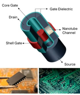
KAUST’s novel architecture relies upon volume-inversion effects to improve performance in multi-gate devices. The volume-inversion effects are introduced when the thickness of the semiconductor film is reduced below the inversion layer thickness induced by the multiple gates.
This technique introduces a number of advantages, including:
- Enhanced number of minority carriers
- Increased velocity saturation
- Increased drain current and transconductance
- Decreased leakage current related power consumption
- This, in turn, improves the performance of current value, sub-threshold slope, and speed.
Why It Is Better
The number of transistors in integrated circuits doubles approximately every 1.5 years. Moore’s Law has proved to be remarkably consistent ever since the invention of the integrated circuit in 1958. For the semiconductor industry to maintain this level of advancement, many design challenges must be overcome. KAUST’s novel FET architecture provides a critical advance, enabling further miniaturization of transistors in integrated circuits. The innovative design offers full-volume inversion, excellent electrostatic control, and ballistic transport. By mitigating short-channel effects, the technology successfully allows an increase in the number of transistors per chip, improving overall performance.
IP Protection
KAUST has several patents pending for this technology.
Invention Track Code
2011-011

Benefits
- Improved performance: Mitigates short-channel effects to allow higher density of smaller transistors, improving device performance
- Faster response: Offers sharper, faster I on/ I off performance than conventional transistors
- Low cost: Can be manufactured less expensively and with higher yields than conventional transistors
- Low power: Offers reduced leakage current resulted power consumption by introducing core-shell gate stacks
- Area efficiency: Can be integrated using ultralargescaleintegration (ULSI) to enable multifunctionality in complex ICs

Applications
This technology will benefit all manner of semiconductor nanoelectronics devices:
- Ultra-mobile computation by introducing high performance mobile devices like iPad, tablets, and smart phones
- Establishing energyefficient, ultralargescaledatahandlingcapable sensor networks