Defect-Free Single Crystal Gallium Nitride Nanolayer
Gallium nitride nanolayer that can be transferred to semiconductor and non-semiconductor substrates
Researchers at KAUST have developed a novel method for forming a defect-free, single crystal gallium nitride (GaN) nanolayer that can be exfoliated and transferred to semiconductor and non-semiconductor substrates for subsequent epitaxy growth of high-quality GaN and its related materials. This high-quality nanolayer is produced using an ultraviolet assisted electrochemical etching technique in a hydrofluoric acid-based electrolyte solution. The dislocation-free GaN layer can be transferred onto a variety of substrates, both hard and flexible, and the layer can act as a seed layer for subsequent epitaxial overgrowth of high-quality GaN. The method has the potential to deliver high-quality GaN-based materials for highly efficient, low-cost optoelectronic and high-power electronic devices.
Technology Summary
Recent successes in the development and optimization of GaN-based materials has led to the ability to produce high-brightness, visible light-emitting diodes, laser diodes, high-density optical storage, and high-powered electronics. However, current methods of producing GaN-based materials are prone to large threading defect densities. There is a market need for the ability of epitaxial films of GaN with low threading defect densities to be grown on various substrates of differing lattice constants and thermal coefficients via a high-throughput, cost-effective and energy-efficient process.
How It Works
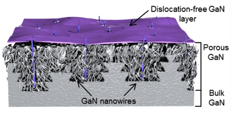
In the developed method, previously fabricated GaN wafers are grown using a metal-organic chemical vapor deposition technique on a sapphire substrate. The electrochemical etching technique in hydrofluoric acid-based electrolyte solution results in the formation of a porous GaN layer. As the sample dries following etching, the thin surface layer collapses downward and sticks to the porous GaN because of water surface tension forces. This sticking would ordinarily make it nearly impossible for a subsequent mechanical exfoliation; however, the researchers dry the GaN samples using a critical point dryer in liquid carbon dioxide. Results based on a transmission electron microscopy and energy dispersive x-ray spectroscopy indicate that the nanolayer consists of a single-crystalline GaN.
Why It Is Better
Current methods of producing GaN nanolayers are based on non-native substrates. This causes the formation of a high grown-in defect density during the epitaxy growth of GaN and its related materials, hence decreasing the quality of the material systems. The synthetic approach produces a thread dislocation-free GaN nanolayer using a simple, inexpensive and energy-efficient ultraviolet-assisted electroless etching technique. The nanolayer that is produced in this way can be transferred to other desired substrates, serving as a seed layer for the subsequent epitaxial growth of dislocation-free, high-quality GaN. Utilization of the invention could enable the production of high-quality optoelectronic and electronic devices.
IP Protection
KAUST has several patents pending for this technology.
Invention Track Code
2013-009

Benefits
- Defect-free, high-quality GaN is produced
- Simple, inexpensive, energy-efficient process
- GaN can be transferred to desired substrates for epitaxial growth of defect-free GaN

Applications
- Semiconductor
- Optoelectronics
- Electronic devices and advanced power applications