An Integrated Lab-on-a-Chip Smart Sensor for Gas Detection
For environmental monitoring and hazard detection applications
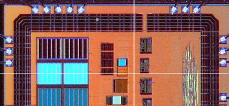
Microphotograph of the first generation chip which has sensing element (IDEs)
and electronic circuitry on same substrate
This novel microsystem will be able to assess indoor and outdoor air pollution and hazardous materials in a compact, reliable, energy-efficient, and cost-effective way. It uses energy-efficient sensor interface circuits and energy harvesting to achieve standalone batteryless sensor nodes.
A gas sensor using a metal organic framework material can be fully integrated with related circuitry on a single substrate. In an on-chip application, the gas sensor can result in an area efficient fully integrated gas sensor solution.
The integrated sensor’s application areas include oil and gas industries, civil defense and public safety organizations.
Technology Summary
Existing gas and vapor detection systems are bulky, expensive, and power hungry, which hinders their wide-scale deployment for continuous environmental monitoring indoors and outdoors. Our innovative microsystem is compact, reliable, energy-efficient, and cost-effective. Integrating the sensor with electronic circuitry on the same die reduces size, weight, cost, and also improves signal transduction. Its superior performance makes it a good candidate to replace existing bulky sensors in oil and gas industries, and in civil defense and public safety applications.
How It Works
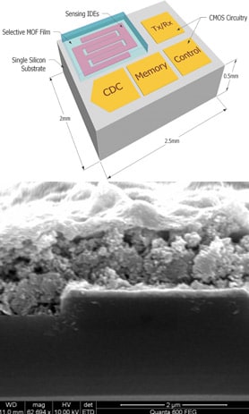 Sensing interdigitated electrodes (IDEs) are built using the top metal layer of standard CMOS process. Electronic CMOS circuitry is implemented with the IDEs on the same substrate (see schematic on first page). MOF film, which works as a selective concentrator, is deposited onto the sensing electrodes and the capacitance of the film is monitored upon exposure to the analyte being studied. The film capacitance is directly digitized using lowpower capacitancetodigital converter (CDC) circuitry. Integrating the sensor with electronic circuitry on the same die offers several advantages, e.g. reduced size, weight, and cost, improved signal transduction, lower power consumption, improved immunity to external noise sources, and the ability to add intelligence to the system, i.e. smart sensor.
IP Protection
KAUST has several patents pending for this technology.
Invention Track Code
2011-121

Benefits
- Reduced size
- Reduced weight
- Low cost
- Improved signal transduction
- Lower power consumption
- Improved immunity to external noise sources

Applications
- Monitoring toxic gases in oil and gas industries
- Wireless gas sensor networks for environmental monitoring over large areas
- Civil defense and public safety